 CM66
CM66
CM66
CM66

Clock Module with built-in receiver, supporting GPS/Beidou, Two frequency output, Holdover better than ±1.5us/24h (△T=±5℃);
Application: Power grid, Clock reference, Base station and High precise server etc.
Standard Model:CM66G-D129-10.00MHz-A
| Parameters | Remark | |
| Type | Auto Position Lock |
Applicable to CM66G and H series | |
| Number of Channels | 50 | ||
| Frequency Band | L1(1575,42MHz) | ||
| Tracking Code | C/A Code | ||
| Tracking Capability | 12 Satellites | ||
|
Sensitivity | Tracking & Navigation -162dBm | ||
| Hot start -157dBm | |||
| Cold start -148dBm | |||
| Antenna INPUT | SMA-KE |
| Parameters | Remark | |
| Type | Auto Position |
Applicable to CM66K and L series | |
| Frequency band |
GPS L1(1575.42Mhz)/ BD2 B1(1561.098MHz) | ||
| Tracking capability | 12 Satellites | ||
| Sensitivity | Tracking -159dBm | ||
| Capturing -144dBm | |||
| Antenna INPUT | SMA-KE |
|
State input | Parameters | Min. | Typ. | Max. | Unit. | Test Condition |
| Lock | 2.7 | V | <5mA Load | |||
| Holdover | 0.4 | V | <5mA Load | |||
| Connector | Pin 8 | |||||
|
GPS 1PPS Reference output | Parameters | Min. | Typ. | Max. | Unit. | Test Condition |
| Waveform | HCMOS | |||||
| High-level Output Voltage | 2.7 | V |
50Ω | |||
| Low-level Output Voltage | 0.4 | V | ||||
| Pulse Width | 100 | ms | ||||
| Connector | Pin 10 | |||||
| State input | Parameters | Min. | Typ. | Max. | Unit. | Test Condition |
| Lock | 2.7 | V | <5mA Load | |||
| Holdover | 0.4 | V | <5mA Load | |||
| Connector | Pin 5 | |||||
|
Holdover | Parameters | Min. | Typ. | Max. | Unit. | Test Condition |
| 24 hrs | -1.5 | 1.5 | μs | △T=±2℃, 24 hours holdover after turning on 7 days and GPS lock 3 days |
|
Supply voltage | Parameters | Min. | Typ. | Max. | Unit. | Test Condition |
| Supply voltage | 4.75 | 5.0 | 5.25 | V | ||
| Current consumption | 2000 | mA | During Warm-up | |||
| 1000 | mA | During steady state operation @25℃ | ||||
| Ac ripple | 50 | mA | 10Hz ~ 1MHz | |||
| Connector | Pin 3 | |||||
|
RF output 1 | Parameters | Min. | Typ. | Max. | Unit. | Test Condition |
| Nominal Frequency | 19.6608 | MHz | ||||
| Waveform | HCMOS | |||||
| High-level Output Voltage | 2.7 | V | <5mA Load | |||
| Low-level Output Voltage | 0.4 | V | <5mA Load | |||
| Rise/Fall Time | 8 | ns | <5mA Load | |||
| Duty Cycle | 45 | 50 | 55 | % | <5mA Load | |
| Accuracy | -1 | +1 | E-12 | 24 hrs average when locked to 1 PPS | ||
| Short-term Stability | 2 | E-11 | Temperature stability, no EMI/EMC or other interference, test after power on for 1 hour ref. to 25℃; 1s, using PN9000 equipment | |||
| Aging Tolerance Per Day | -2 | +2 | E-10 | Vcc, TA constant measurement referenced to frequency observed with TA=25℃, Vcc=5.0V, in FREE RUN condition and after 30 days of operation. | ||
| Aging Tolerance Per Year | -1 | +1 | E-8 | |||
|
Phase noise | -90 | dBc/Hz | @10Hz offset | |||
| -120 | dBc/Hz | @100Hz offset | ||||
| -140 | dBc/Hz | @1KHz offset | ||||
| -150 | dBc/Hz | @10KHz offset | ||||
| -155 | dBc/Hz | @100KHz offset | ||||
| -155 | dBc/Hz | @1MHz offset | ||||
| Connector | Pin 2 | |||||
|
RF output 2 | Parameters | Min. | Typ. | Max. | Unit. | Test Condition |
| Nominal Frequency | 61.44 | MHz | ||||
| Waveform | Sine wave | |||||
| Amplitude | 6 | 10 | dBm | |||
| Load | 50 | Ω | ||||
| Harmonic | -30 | dBc | ||||
| Stray | -60 | dBc | ||||
| Accuracy | -1 | +1 | E-12 | 24 hours average when lock to 1 PPS | ||
| Short-term stability | 2 | E-11 | Temperature stability, no EMI/EMC or other interference, test after power on for 1 hour ref. to 25℃; 1s, using PN9000 equipment | |||
| Aging Tolerance Per Day | -2 | +2 | E-10 | Vcc, TA constant measurement referenced to frequency observed with TA=25℃, Vcc=5.0V, in FREE RUN condition and after 30 days of operation. | ||
| Aging Tolerance Per Year | -1 | +1 | E-8 | |||
|
Phase noise | -80 | dBc/Hz | @10Hz offset | |||
| -110 | dBc/Hz | @100Hz offset | ||||
| -130 | dBc/Hz | @1KHz offset | ||||
| -145 | dBc/Hz | @10KHz offset | ||||
| -150 | dBc/Hz | @100KHz offset | ||||
| -155 | dBc/Hz | @1MHz offset | ||||
| Connector | Pin 14 | |||||
|
PP2S Output waveform feature | Parameters | Min. | Typ. | Max. | Unit. | Test Condition |
| Waveform | HCMOS | |||||
| High-level Input Voltage | 2.7 | V |
50Ω | |||
| Low-level Input Voltage | 0.4 | V | ||||
| Pulse Width | 10 | μs | ||||
| Phase | Synchronous with 19.6608MHz falling edge in even second of 1PPS | |||||
| Connector | Pin 12 | |||||
|
Serial Interfaces | Parameters | Min. | Typ. | Max. | Unit. | Test Condition |
| Rx High-level Input Voltage | 2.7 | V | ||||
| Rx Low-level Input Voltage | 0.4 | V | ||||
| Tx High-level Output Voltage | 2.7 | V | ||||
| Tx Low-level Output Voltage | 0.4 | V | ||||
| Data format | NMEA-0183 | |||||
| Serial protocol | 9600-N-8-1 | |||||
| Connector | Pin 6 and Pin 7 | |||||
|
Environmental Compliance | Parameters | Conditions |
| Operating temperature | -20℃~ 75℃ | |
| Storage temperature | -55℃~ 105℃ | |
| Storage humidity | 30% ~ 80% | |
| ESD level | Human Body Model, class 2: 2000V to 4000V; ANSI/ESDA/JEDEC JS-001-2-2010. | |
| Human Body Model, class B: 200V to 400V; ANSI/ESDA/JEDEC JS-001-2010. | ||
| Moisture Sensitivity Level | Not humidity sensitive |
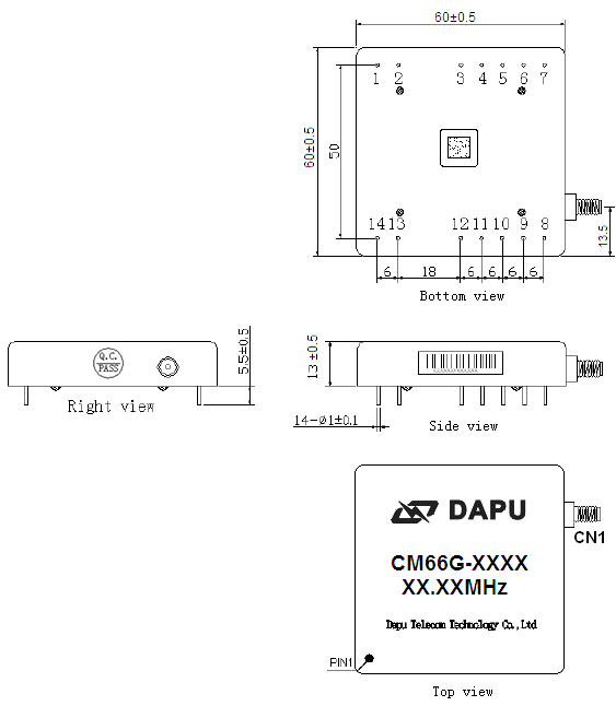
| PIN DEFINITION | |||
| PIN | NAME | DESCRIBTION | |
| 1 | GPS_BCKP | GPS receiver backup battery, supply 1.4V to 3.6V, if not use, please connect to GND | |
| 2 | 19.6608MHz output | 19.6608MHz OCXO output | |
| 3 | VCC | Supply voltage 4.75V~5.25V | |
| 5 | State output | State output. Output high level when the CM is locked and stable, others low level | |
| 6 | RX input | Asynchronous serial data input , 9600-N-8-1. | |
| 7 | TX output | Asynchronous serial data output , 9600-N-8-1. | |
| 8 | State INPUT | H: Lock | The work state is set to normal operation when the state input is high |
| L: Holdover | The work state is set to hold over when the state input is low | ||
| 10 | GPS 1PPS Input | Clock module PP1S output | |
| 12 | PP2S | Clock module PP2S output | |
| 14 | 61.44MHz output | 61.44MH output | |
| 4、9、11、13 | GND | GND | |