 CM55
CM55
CM55
CM55
Small size, Low height, Holdover better than ±1.5us/24h(△T=±10℃);
Application: Power grid, Clock reference, Base station, High precise server etc.
Feature:
1.5μs holdover for 24 hrs, ultra thin, high cost effective, applied to a relatively stable temperature environment
|
1 PPS Reference input | Parameters | Min. | Typ. | Max. | Unit. | Test Condition |
| Waveform | HCMOS | |||||
| High-level Output Voltage | 2.7 | V |
50Ω | |||
| Low-level Output Voltage | 0.4 | V | ||||
| Pulse Width | 10 | μs | ||||
| Connector | Pin 10 | |||||
|
State input | Parameters | Min. | Typ. | Max. | Unit. | Test Condition |
| Lock | 2.7 | V | <5mA Load | |||
| Holdover | 0.4 | V | <5mA Load | |||
| Connector | Pin 8 | |||||
|
RF Output | Parameters | Min. | Typ. | Max. | Unit. | Test Condition | ||||||
| Frequency | 10 | MHz | ||||||||||
| Waveform | HCMOS | |||||||||||
| High-level Output Voltage | 2.7 | V | <5mA Load | |||||||||
| Low-level Output Voltage | 0.4 | V | <5mA Load | |||||||||
| Rise/Fall Time | 8 | ns | <5mA Load | |||||||||
| Duty Cycle | 45 | 50 | 55 | % | <5mA Load | |||||||
| Accuracy | -1 | +1 | E-12 | 24 hours average when lock to 1 PPS | ||||||||
| Short-term stability | 2 | E-11 | Temperature stability, no EMI/EMC or other interference, test after power for 1 hour ref. to 25℃; 1s, using PN9000 equipment | |||||||||
| Aging Tolerance Per Day | -2 | +2 | E-10 | Vcc, TA constant measurement referenced to frequency observed with TA=2525℃, Vcc=5.0V, in FREE RUN condition and after 30 days of operation. | ||||||||
| Aging Tolerance Per Year | -1 | +1 | E-8 | |||||||||
|
Phase noise | -118 | dBc/Hz | @10Hz offset | |||||||||
| -138 | dBc/Hz | @100Hz offset | ||||||||||
| -148 | dBc/Hz | @1KHz offset | ||||||||||
| -150 | dBc/Hz | @10KHz offset | ||||||||||
| -150 | dBc/Hz | @100KHz offset | ||||||||||
| -150 | dBc/Hz | @1MHz offset | ||||||||||
| Connector | Pin 14 | |||||||||||
| Holdover Capability | Holdover Time | Min. | Typ. | Max. | Unit. | Test Condition | ||||||
| 24 hours | -1.5 | 1.5 | μs | △T=±10℃, 24 hours holdover after turning on 7 days and GPS lock 3 days | ||||||||
|
Supply Voltage | Parameters | Min. | Typ. | Max. | Unit. | Test Condition |
| Supply Voltage | 4.75 | 5.0 | 5.25 | V | ||
| Current consumption | 1400 | mA | During warm-up | |||
| 600 | mA | During steady state operation @25℃ | ||||
| AC ripple | 50 | mA | 10Hz ~ 1MHz | |||
| Connector | Pin 3 | |||||
|
1PPS Output Waveform Features | Parameters | Min. | Typ. | Max. | Unit. | Test Condition |
| Waveform | HCMOS | |||||
| High-level Output Voltage | 2.7 | V |
50Ω | |||
| Low-level Output Voltage | 0.4 | V | ||||
| Pulse Width | 10 | μs | ||||
| Connector | Pin 12 | |||||
|
State intput | Parameters | Min. | Typ. | Max. | Typ. | Test Condition |
| Lock | 2.7 | V | <5mA Load | |||
| Holdover | 0.4 | V | <5mA Load | |||
| Connector | Pin 5 | |||||
|
Serial Interfaces | Parameters | Min. | Typ. | Max. | Typ. | Test Condition |
| Rx high-level input voltage | 2.7 | V | ||||
| Rx low-level input voltage | 0.4 | V | ||||
| Tx high-level output voltage | 2.7 | V | ||||
| Tx low-level output voltage | 0.4 | μs | ||||
| Serial protocol | 9600-N-8-1 | |||||
| Connector | Pin 6 and Pin 7 | |||||
|
Environment Compliance | Parameter | Conditions |
| Operating temperature | -20℃~ 75℃ | |
| Storage temperature | -55℃~ 105℃ | |
| Storage humidity | 30% ~ 80% | |
| ESD level | Human Body Model, class 2: 2000V to 4000V; ANSI/ESDA/JEDEC JS-001-2-2010. | |
| Human Body Model, class B: 200V to 400V; ANSI/ESDA/JEDEC JS-001-2010. | ||
| Moisture Sensitivity Level | Not humidity sensitive |
Vibration
Test Condition:
Amplitude: 0.75mm;acceleration: 10g;10Hz~500Hz; a cycle per 30min, test for 2 hours in 3 directions
(3 directions: X, Y and Z), IEC 68-2-06 Test Fc.
Shock
50g;11ms;half sine wave (3 directions: X, Y and Z), IEC 68-2-27 TestEa/Severity 50A.
Mechanical Structure (mm)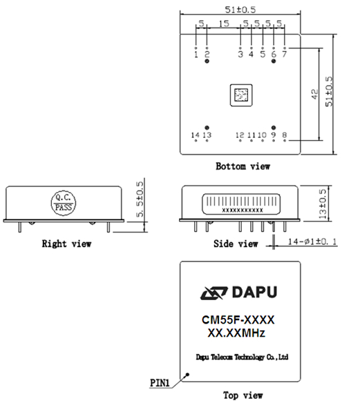
Note 1: Tolerance ±0.2mm without marking
Note 2: Referential weight 51.4g
| PIN DEFINITION | |||
|---|---|---|---|
| PIN | NAME | Power supply input, 4.75V ~5.25V. | |
| 3 | VCC | DESCRIBTION | |
| 5 | State Output | State output. Output high level when the CM is locked and stable, others low level. | |
| 6 | RX INPUT | Asynchronous serial data input. 9600-N-8-1 | |
| 7 | TX OUTPUT | Asynchronous serial data output. 9600-N-8-1 | |
| 8 | State INPUT | H: Lock | The work state is set to normal operation when the state input is high |
| L: Holdover | The work state is set to hold over when the state input is low. | ||
| 10 | 1PPS INPUT | 1PPS reference input | |
| 12 | 1PPS OUTPUT | Clock module 1PPS output | |
| 14 | 10MHz OUTPUT | 10MHz OCXO frequency output | |
| 1、2、9 | NC | hang in the air | |
| 4、11、13 | GND | GND | |